On Sun, Dec 23, 2007 at 05:08:55AM +0100, Igor2 wrote:
> On Sat, 22 Dec 2007, DJ Delorie wrote:
>
> >
> >>    http://ad7gd.net/geda/panelusb-sm.jpg
> >
> >Am I the only one who tries to make the absolutely smallest board I
> >can still fit my parts on?  My latest board would fit in the blank
> >spots between your chips.
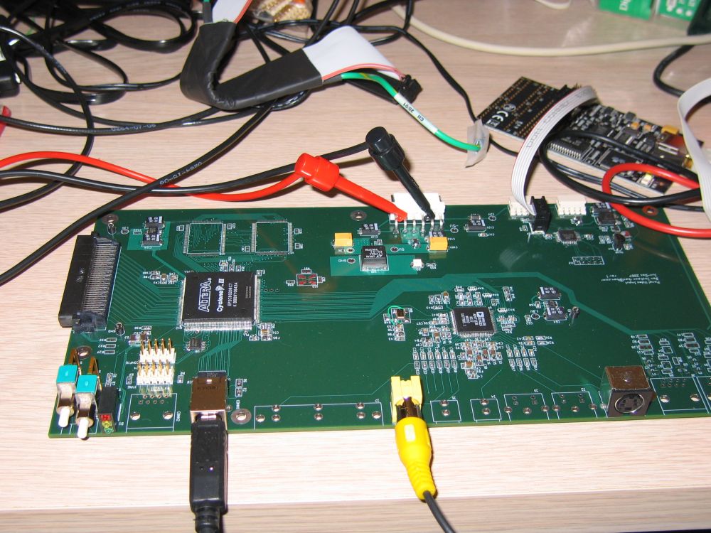
Most of the size of the board is due to the width.  Those edge
connectors (in the photo it's the near side) will actually be exposed
from the device when it's done.  The connectors on the far side and
the left are internal.  It could have been narrower, but not enough
to significantly change the price.  Not to mention the layout started
with a fixed price for 60 square inches.

Big area made it easy to keep the analog section away from the digital
noise, too.

> Btw, how do you guys solder those big SM chips with so many pins?

That's the funny thing.  The soldering on the QFPs is so much nicer
than most of the 0603s because I do it bathed in flux.  You just line up
the chip, tack two corners, and then use the tip of your iron to drag
a tiny ball of solder slowly along the pins.  For the 0.5mm stuff I take
no chances and I bathe it in liquid flux (and add more if I get any
solder bridges).  For fatter stuff (0.65mm or 0.8mm ) I'll just slather
on flux with the pen.  The downside is that I have to wash the board
after using the liquid flux, but it's worth it.

John Griessen wrote:
> Hey, that's a lot of function you got going!

Well heck, I'm a software guy.  Now that I have the board, it's all
downhill!

BTW, I've decided that 0.1u caps are the hardware equivalent of
semicolons...  There are 128 caps on that board and 79 are .1u.
And I'm totally relieved to see decent picture quality out of the
ADV7183B, since I followed their zillion-cap recommendations to the
letter.

--
Ben Jackson AD7GD
<[EMAIL PROTECTED]>
http://www.ben.com/


_______________________________________________
geda-user mailing list
geda-user@moria.seul.org
http://www.seul.org/cgi-bin/mailman/listinfo/geda-user