One of the remaining components on my DSO board are the
DC/DC-Converters. I have a few of them, and I have to do the layout
carefully to avoid noise.
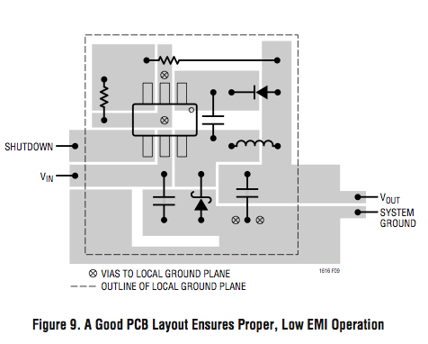
In some datasheets layout examples are available similar to this
picture:

http://www.mikrocontroller.net/attachment/44284/Bild_1.png

I think I can make the copper areas with PCB polygons. But the pads of
the components will not touch the copper polygons by default. I wonder
if I should connect the pads to polygons by traces, or if I should
reduce the clearance of the pads for full contact. The later may make
hand soldering difficult.

I think this type of layout would be easier if we would have "negative
traces" so that we could draw one large copper rectangle and cut it in
pieces by negative traces.

Just found a nice paper of DC/DC-Converter layout principles, if someone
is interested:

http://www.edn.com/contents/images/6347258.pdf


_______________________________________________
geda-user mailing list
geda-user@moria.seul.org
http://www.seul.org/cgi-bin/mailman/listinfo/geda-user