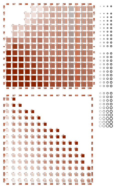
I discovered that my printer "bloats" traces by a pixel or so when
printed, and my crude attempts at etching didn't result in traces that
were the same width as designed.  So, I added an option to the
postscript HID that lets you compensate for these deviations.
I.e. you can, at print time, make all traces/pads/pins/vias slightly
thicker or narrower than "actual" so that the resulting board ends up
with the right sizes.
I've put a calibration board file at http://www.delorie.com/pcb/ that
has a wide range of tiny traces and gaps with various bloat
adjustments so anyone who wants to can both calibrate their process
and find out how small they can go before the error rate becomes
problematic.

There's a PNG of the board so you know what it's supposed to look
like: http://www.delorie.com/pcb/bloat.png

FYI I discovered all this with a 200x IntelPlay USB microscope :-)