On Tue, 23 Aug 2011 02:41:53 -0700
Andrew Poelstra <as...@sfu.ca> wrote:
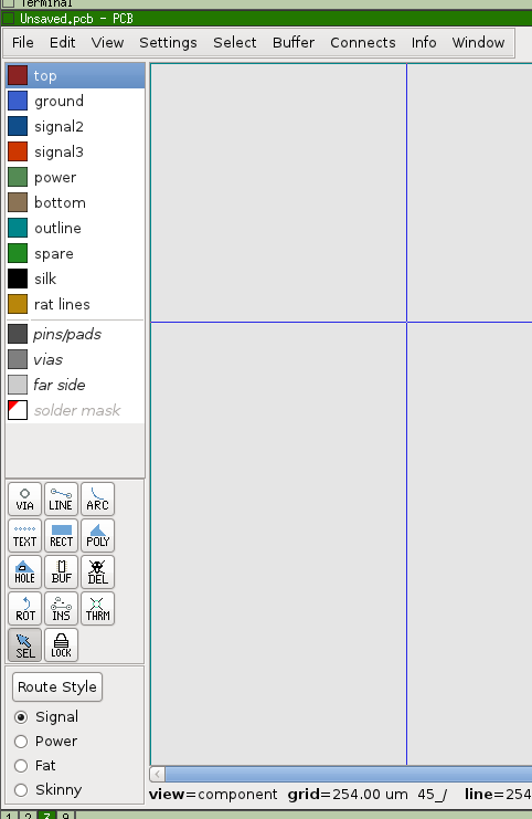
> On Tue, Aug 23, 2011 at 02:22:25AM +0200, Kai-Martin Knaak wrote:
> > Andrew Poelstra wrote:
> >
> > > I have implemented the italicized/separated
> > > suggestion. You can see it here:
> > >
> > > http://www.wpsoftware.net/andrew/dump/mockup4.png
> >
> > Nice.
> > I note, that the longest layer name is "solder mask". Why not
> > shorten it to "mask" to save screen estate for the canvas?
> >
>
> I'd be cool with this, but "solder mask" is a well-known phrase
> in the industry. It has a definition on Google and a Wikipedia
> page.
>
> "mask" has nowhere near the same information content. IMHO, it
> is not worth the space savings. Maybe "s.mask" would be better?

Perhaps it would be best to make the displayed name of the solder mask
layer a user preference.  Also, it would be nice to give the user
control over the layer name font size:  then a user could choose a
small font.  My general system font is too big for use in pcb, where I
really want maximum screen real estate available for the board.  I
found the lesstif GUI uses more reasonable (i.e., smaller) font
sizes on my Ubuntu system.

Regards,
Colin


_______________________________________________
geda-user mailing list
geda-user@moria.seul.org
http://www.seul.org/cgi-bin/mailman/listinfo/geda-user